AD7705 General Description
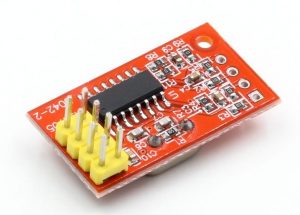
AD7705 is a complete 16-bit, low-cost, Σ-Δ analog-to-digital converter suitable for dc and low-frequency ac measurement applications. It uses sigma-delta technology to obtain 16-bit error-free data output. Its low power consumption (1 mW max at 3 V) allows it to be used in loop-powered, battery-powered, or locally powered applications. An on-chip programmable gain amplifier provides gain settings from 1 to 128 and accepts both low-level and high-level analog inputs without the use of external signal conditioning hardware.
AD7705 has the characteristics of high resolution, wide dynamic range, self-calibration, excellent anti-noise performance, and low voltage and low power consumption, which is suitable for the needs of microcomputer signal processing in weighing systems. It has a programmable gain amplifier with a gain range of 1 to 128, which can be directly connected to the pressure sensor. It uses an asynchronous serial SPI interface and can be directly connected to the hardware SPI interface of the AVR microcontroller.
AD7705 is very suitable for applications in instrument measurement, industrial control, and other fields.
AD7705 Pin Configuration and Function Description
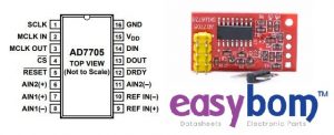
AD7705 Pinout
SCLK: Serial interface clock input.
MCLK IN: Chip working clock input. It can be a crystal oscillator or an external clock with a frequency range of 500kHz to 5MHz.
MCLK OUT: Clock signal output. When the crystal oscillator is used as the working clock of the chip, the crystal oscillator must be connected between MCLK IN and MCLK OUT. If an external clock is used, MCLK OUT can be used to output an inverted clock signal as a clock source for other chips. This clock output can be turned off by programming.
CS: Chip Select, active low.
RESET: Chip reset port. When this terminal is low, the interface logic, self-calibration, data filter, etc. in the AD7705/AD7706 chip are all powered on.
AIN1( + ), AIN1( – ): are the positive and negative ends of the first differential input channel, respectively.
AIN2( + ) , AIN2( – ): are the positive and negative ends of the second differential input channel, respectively.
REF IN( + ) , REF IN( – ): are the positive and negative ends of the reference voltage, respectively.
DIN: Serial data input terminal.
DOUT: Conversion result output terminal.
DRDY: A/D conversion end flag.
VDD: Supply Voltage. 2.7 V to 5.25 V operation.
AIN3: Negative Input of the Differential Analog Input Pair AIN2(+)/AIN2(−) for AD7705.
GND: Ground Reference Point for the AD7705 Internal Circuitry.
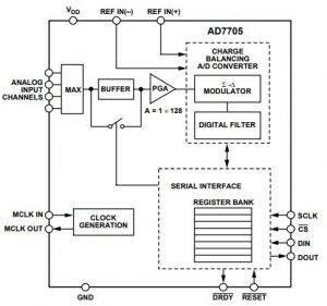
AD7705 Functional Block Diagram
How to Use AD7705
The AD7705 is a complete 16-bit A/D converter. In application, only need to connect crystal oscillator, precision reference source, and a small amount of decoupling capacitor for continuous A/D conversion. The following briefly introduces its working principle and characteristics.
2.1 Programmable gain amplifier and effective resolution
The on-chip gain programmable amplifier PGA of AD7705 can select one of eight kinds of gain, such as 1, 2, 4, 8, 16, 32, 64, 128, etc., and can use it to amplify various input signals of different amplitude ranges to close to the full-scale voltage of the A/D converter, and then A/D conversion. No amplifier circuit is used in this application circuit, so it is beneficial to improve the conversion quality. When the power supply voltage is 5V and the reference voltage is 2.5V, the AD7705 can directly accept unipolar signals with a swing range from 0 to +20mV to 0 to +2.5V and bipolar signals from 0 to ±20mV to 0 to ±2.5V. It must be pointed out that the negative voltage here is relative to the AIN(-) or COMMON pins, so these two pins should be biased to the appropriate positive potential.
When the input analog signal is continuously sampled by the A/D converter, its output update rate is programmable. It should be noted that the faster the output is updated, the lower its effective resolution, but not less than 13-bit effective resolution.
-
2 Read and write timing
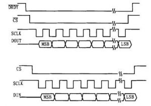
The AD7705 can interface directly with the AT89C51. The data lines used include a chip select CS, serial clock input SCLK, command or data input DIN, and conversion result output DOUT, etc. Only when the status signal DRDY indicates that the data of the output data register is ready, the microcontroller can read the conversion result. Figure 2 and Figure 3 show the timing diagrams of the read and write data cycles, respectively.
- 3 On-chip registers
The AD7705 contains eight registers. All operations on the chip must first start by writing to the communication register. After power-on or reset, the waiting command data of the chip is written into the communication register.
Where to use AD7705
Due to its characteristics of dual-channel, low cost, and high resolution, ADC AD7705 is ideally used in industrial and process-control applications.
- Pressure measurement using the AD7705
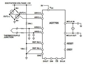
As the figure below shows, the AD7705 is used with a pressure transducer which is arranged in a bridge network and used to provide a differential output voltage between the terminals of OUT (+) and OUT (-). When a rated and full-scale pressure (eg. 300 mmHg) is imposed on the transducer, the differential output voltage is 3 mV/V of the input voltage between the terminals of IN (+) and IN (-). The variations in the excitation voltage will not cause errors in the system because it can generate the reference voltage for AD7705.
- Smart transmitter using the AD5507
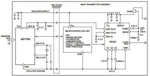
Depending on its specific characteristics, the AD5507 can also be used in smart transmitters. Due to the fact that the smart transmitter must operate from a 4 to 20 mA loop with a tolerance of 0.5mA, the transmitter is able to operate with the minimum current of 3.5 mA. As a result of its feature of low power consumption, the AD5507 only consumes 320 μA when operating. Thus at least 3mA is left for the rest of the transmitter.
- Battery Monitoring using the AD5507
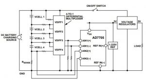
In various portable equipment, the application of battery monitoring must make use of the specific characteristics of the AD5507 to measure differentially the voltage across a single cell. Its dual input channels are ideally used to monitor the voltage and current. The RSENSE can be kept low due to the fact that the AD5507 is able to accommodate extremely low input signals so as to reduce undesired power dissipation. In addition, the AD5507 can be used to achieve a much higher level of resolution due to its relatively better noise performance compared with the integrating ADCs. With a gain of 128, a ±9.57 mV full-scale signal can be measured with a resolution of 2 μV, giving 13.5 bits of flicker-free performance in such a system.
AD5507 Application Notes
- Timing points: when the digital interface is lost, the digital interface of AD7705 can be reset by a high level of ADIN input for more than 32 pulse cycles (DCLK). It will not affect any registers inside AD7705, all registers will keep the contents before reset, but the contents of all registers are uncertain when the digital interface is lost, so it is strongly recommended to reset all registers inside AD7705 after reset, Prevent mistakes.
- When the AD7705 clock is greater than 2M, the CLK bit of the clock setting register should be set to 1, and it should be set to 0 when it is less than 2M.
- The DRDY signal is an indication signal that the AD conversion of data is completed. During the low-level period, it indicates that the AD conversion is completed, and the content of the data register can be read. During the high-level period, it indicates that the AD conversion is in progress, and the data register cannot be accessed at this time.
- Whether it is calibration or data AD conversion, the digital filter synchronization bit FSYNC must be set to 0 so that the calibration or data AD conversion of AD7705 can be performed.
- When using the non-buffering mode, the change of the resistance and capacitance of the AD7705 analog input front end has a great influence on the AD conversion accuracy.
- Voltage input range: For unbuffered mode, the analog input signal range is between GND-30mV and VDD+30mV. For buffer mode, the analog input signal range is from GND+50mV to VDD-1.5V.
AD7705 Datasheet Download
Look through the AD7705 Datasheet to have a deep insight into it, thus avoiding some troubles caused by unfamiliarity when engineers conduct an electronic project related to it.
Conclusion
In this article, Easybom has introduced elaborately the AD7705, including its application, working principle, pinout, and more. We hope that you can benefit a lot from this article about this electronic component which gives you some instructions on related projects.