AD623 General Description
AD623 is an integrated single-supply instrumentation amplifier that can provide full-supply amplitude output from one power source (+3V from +12V). It permits gain programming using one gain setting resistor, which gives you more flexibility. The low power consumption, the large voltage ranges for supply, and a complete output amplitude of the supply make the AD623 ideal to operate a battery. It is able to replace discrete instrumentation amplifiers, and it provides excellent linearity even in the smallest of spaces and stable temperature stability.
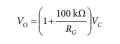
The AD623 reduces the number of errors down its excellent AC common-mode rejection (AC CMRR) which increases with increasing gain. The line noise, as well as harmonics, remain constant for up 200Hz thanks to CMRR. It can still provide excellent performance when using dual supply (2.5 -6V). The full-supply amplifier output stage increases the dynamic range even with a low voltage supply. It conforms to the industry-standard configuration with 8 pins. The AD623 has one gain (G=1) without the need for external resistors. When the resistor has been connected to the AD623, it will be programmed to adjust the gain. In addition, the gain could be as high as 1000 times.
Due to its exceptional performance, the AD623 is frequently employed in low-power medical equipment Sensor interface, thermocouple amplifier industry process control, differential amplifier, and data acquisition with low power.
AD623BN Specification
The voltage of the supply is 5V.
Current (supply) the following: 3375mA
The rate of slew: 0.3V/ms
Current – input bias: 17nA
Voltage – Supply, single/dual (+-): 2.7V~12V + 2.5V~6V
Negative Supply Voltage-nom (Vsup) (Vsup): -5V
Average bias current-max (IIB): 0.0275mA
Limit of supply voltage 6V
Voltage Input offset 25mV
-3db bandwidth: 800kHz
Neg voltage of supply – maximum (Vsup) (Vsup): -6V
Current-max of input offset (IIO): 0.002mA
Voltage gain-min 1
Common-mode reject ratio-min: 77 dB
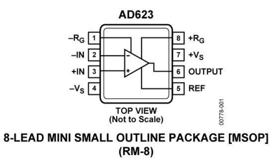
AD623BN Pin Configuration
AD623BN Instruction
How to Use
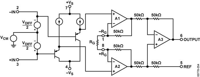
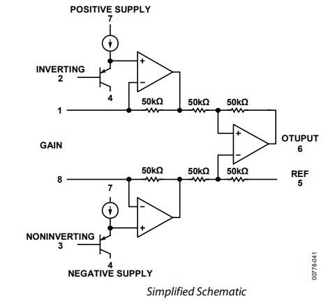
AD623BN is an integrated instrumentation amplifier that is able to operate under single or dual supply even at common-mode voltages at the negative supply rail. The PNP transistors are used as voltage buffers and are used to provide a common-mode signal to the input amplifiers. The input signal is applied to them. The resistor of 50kΩ applied in each amplifier feedback assures gain programmability.
The differential output is
The differential voltage is then converter to a single-ended voltage using the output amplifier, which also rejects any common-mode signal at the output of the input amplifiers.
The amplifiers can swing to either supply rail, as well as have their common-mode range extended to below the negative supply rail, the range over which the AD623 can operate is further enhanced.
The output voltage at Pin 6 is measured with respect to the potential at Pin 5. The impedance of the reference pin is 100 kΩ; therefore, in applications requiring V/I conversion, a small resistor between Pin 5 and Pin 6 is all that is needed.
Note that the bandwidth of the in-amp decreases as the gain is increased. This occurs because the internal op-amps are the standard voltage feedback design. At unity gain, the output amplifier limits the bandwidth.
Where to Use
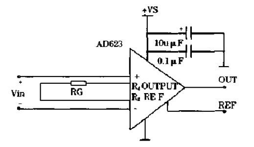
(1) Dual power supply applications. Figure 1(a) shows the basic circuit for a dual power supply application. Capacitors (preferably surface-mounted ceramic chip capacitors) and 10uF capacitors (preferably tantalum electrolytic capacitors) are connected to the positive and negative power supply pins.
(2) Single-supply applications. Figure 1(b) shows the basic circuit for a single-supply application. The capacitors (preferably surface-mounted ceramic chip capacitors) and 10uF capacitors (preferably tantalum electrolytic capacitors) are connected to the power pins.

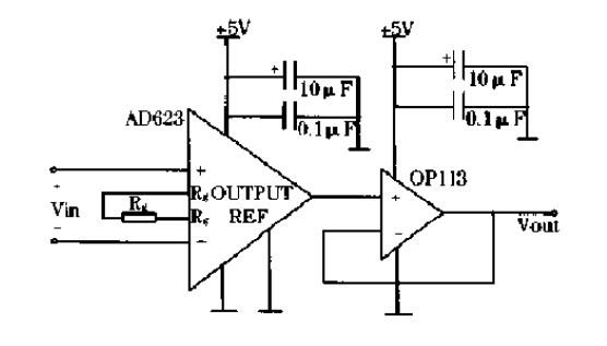
(3) AD623 works in the way of OP113
AD623 is equipped with a clamping diode based on the power supply, so that the input end, output end, reference end, and gain adjustment end can safely withstand higher or lower overvoltages.
The AD623 is designed to drive a load of 10kΩ or more. If the load is less than 10kΩ, a precision single op-amp such as OPll3 should be used as a buffer to improve the drive capability, as shown in the figure below. At this time, when the load is as small as 600Ω, the output swing of 0-4V can be obtained on the load.
(4) AD623 working in a bipolar signal data acquisition system in a single power supply mode
The figure below is an application example of AD623 working in a bipolar signal data acquisition system in a single power supply mode
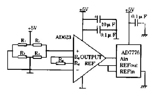
In practical applications, it is often encountered that the bipolar signal is amplified and then sent to the ADC for A/D conversion, which requires the bipolar signal to be converted into the effective input range of the ADC. The figure below uses the reference voltage of AD623 A good solution to this problem. In the figure, the bridge is powered by 5V. Therefore, the full-scale output voltage of the bridge (±10mV) has a common-mode voltage of 2.5V. AD623 removes the common-mode component and amplifies the differential mode signal (±10mV) by 100 times to generate a ± 1V output signal, in order to make this output signal within the effective input range of AD7776, it must be increased by at least 1V. In this example, it is increased by 2V, and the 2V voltage adopts the 2V reference voltage of AD7776. In this way, the analog voltage entering the input terminal of AD7776 is 2±1V, which is just within the effective input range of AD7776.
(5) Amplifying low common-mode voltage signals
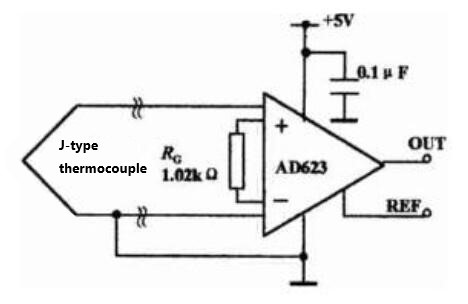
Since the common-mode input range of the AD623 can be extended to 0.1V below ground, it is possible to measure small differential signals with low or no common-mode components. The figure below is an application of a thermocouple, one end of the J-type thermocouple is grounded. Over the temperature range of -200°C to +200°C, the J-type thermocouple provides a voltage range from -7.890mV to 10.777mV, the AD623 is programmed with a gain of 100 (RG=1.02kΩ), and 2V is applied to the REF pin, resulting in output voltages ranging from 1.110V to 3.077V relative to the ground
Datasheet
https://pdf.easybom.com/r/datasheets/rochesterelectronicsllc-ad625ad-datasheets-5020.pdf
Manufacturer
Rochester Electronics ranks as a global leading semiconductor provider. Due to their products’ characteristics of high quality and durability, these products are suitable for long-term production and maintenance in the fields of industry, transportation, and high-reliability markets. Their large inventory includes more than 100,000 products and 15 billion units, making them exceed other companies in terms of selection, capabilities, or solutions.
More About : Tech Bable