Printed Circuit Boards (PCBs) have come a long way, progressing from simple single or double-layer boards to more complex multilayer configurations. One popular choice in this evolution is the 6-layer PCB, which efficiently accommodates increased component density and interconnectivity. This article aims to explore the details of a 6-layer PCB stack-up, covering its configuration, considerations, and the manufacturing processes involved.
6-Layer PCB Stack-up Configuration
The configuration of a 6-layer PCB stack-up is crucial for optimal performance and reliability. Here are the key elements in its design:
Layer Sequence
A 6-layer PCB follows a sequence of numbered conductive copper layers:
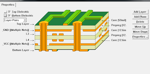
Layer 1: Top/Component layer
Layer 2: Reference plane 1
Layer 3: Signal/Plane layer 2
Layer 4: Signal/Plane layer 3
Layer 5: Reference plane 2
Layer 6: Bottom layer
Top and bottom layers are mainly used for component placement and routing, while the inner layers serve for signals and reference planes.
Reference Plane Placement
For controlled impedance, it is essential to place reference planes (ground and power) adjacent to routing layers. A continuous ground plane beside signals is highly recommended.
Plane Splits
Reference planes can be divided into analog and digital power sections to provide clean isolated supplies to sensitive analog circuits.
Symmetry
A symmetrical arrangement with reference planes above and below the mid-layer offers optimal signal integrity. Asymmetrical stack-ups are also utilized when needed.
Signal Routing
Critical high-speed or noise-sensitive signals should be routed on inner layers sandwiched between planes, avoiding routing on outer layers.
Breakout Vias
Breakout or stub vias are essential when routing inner layer traces to outer layers to confine any stub effects.
Minimum Spacing
Adhering to the board fabricator’s design rule check (DRC) guidelines for minimum trace width, spacing, and annular rings is crucial.
Common 6-Layer Stack-up Arrangements
1. Symmetrical Arrangement
Layer 1: Signal
Layer 2: Ground
Layer 3: Signal
Layer 4: Power
Layer 5: Signal
Layer 6: Ground
Layer 7: Signal
Features:
Identical reference planes above and below the mid-layer.
Excellent signal integrity performance.
Widely used for digital, analog, and RF designs.
2. Asymmetrical Arrangement
Layer 1: Signal
Layer 2: Ground
Layer 3: Signal
Layer 4: Power
Layer 5: Power
Layer 6: Ground
Layer 7: Signal
Features:
Permits splitting power planes into sections.
Discontinuous ground planes may affect signal quality.
Used when power distribution needs warrant it.
3. Hybrid Arrangement
Layer 1: Signal
Layer 2: Ground
Layer 3: Signal
Layer 4: Ground
Layer 5: Power
Layer 6: Ground
Layer 7: Signal
Features:
Top and bottom ground planes for signals.
Mid power plane for splitting.
Balances signal integrity and power needs.
6-Layer PCB Stack-up Thickness Considerations
The overall thickness of a 6-layer PCB depends on various factors:
Copper Layer Thickness
Outer layers: 1 oz (35 μm)
Inner layers: 1 oz or 0.5 oz (18 μm)
Plane layers: 2 oz (70 μm) recommended
Heavier copper allows higher current carrying capacity.
Dielectric Layer Thickness
Typical dielectric layer thickness: 8 mil to 14 mil per layer (112-170 μm glass epoxy FR4 material)
Thinner dielectrics help minimize layer-to-layer capacitance.
Lamination Cycles
A 6-layer board can be fabricated through 2 or 3 lamination cycles.
2 lamination cycles result in lower thickness variation compared to 3 cycles.
Example 6-Layer PCB Stack-up Thickness
Here’s a sample 6-layer PCB stack-up with typical thickness values:
Layer 1 (Top Signal): 1 oz (35 μm)
Layer 2 (Ground): 2 oz (70 μm)
Layer 3 (Signal): 1 oz (35 μm)
Layer 4 (Signal): 1 oz (35 μm)
Layer 5 (Power): 2 oz (70 μm)
Layer 6 (Bottom Signal): 1 oz (35 μm)
Dielectric: 10 mil (254 μm)
Total Thickness (6 Layers): 110 mils (2.79 mm)
This symmetrical arrangement results in approximately 110 mils (2.79 mm) total board thickness. Adjustments in dielectric or copper thickness can be made to achieve specific requirements.
6-Layer PCB Design and Manufacturing Process
The process of assembling a 6-layer PCB involves several stages:
1. Design
Create schematic, layout, and stack-up in PCB design software.
Floorplan components, route traces, and assign plane layers.
Conduct design rule checks (DRC) and signal integrity simulations.
Panelization and generation of Gerber and drill files.
2. Fabrication Data
Board fabricator reviews layer stack-up, material selection, trace widths, spacing, annular rings, hole sizes, drill data, and test points.
Panel drawing, breakaway tabs, and fiducials are considered.
3. Inner Layer Processing
Coat photosensitive dry film on copper-clad laminate.
Expose dry film with a circuit pattern using artwork or laser.
Develop and strip to form the desired copper pattern.
Etch away unwanted copper and remove resist coating.
Clean and prepare layers for lay-up.
4. Lay-Up
Stack material layers according to the 6-layer sequence.
Align layers precisely using fixtures and tooling pins.
Lay-up can be symmetrical or asymmetrical.
2 or 3 lamination cycles are followed.
5. Lamination
Layers are bonded using high pressure and temperature.
Adhesive prepregs melt, flow, and cure to form a multilayer structure.
Layers are bonded with intermediate dielectric.
Autoclave, hydraulic, or thermal press methods are used.
6. Outer Layer Processing
Drill holes for vias using NC drill machines.
Plate copper in hole walls to form barrel interconnects.
Pattern outer layers using a similar imaging process.
Strip/etch to form signal layers with pads/traces.
7. Solder Mask & Silkscreen
Apply Liquid Photoimageable Solder Mask (LPSM).
Expose and develop to form solder masking.
Silkscreen layer is printed for component legends.
8. Surface Finish
Exposed copper is plated with finishes like HASL, ENIG, or Immersion Tin.
Provides solderability and protects copper traces.
9. Routing and Scoring
Individual boards are routed from the larger panel.
V-grooves or milling may be used.
Inspect and clean the PCBs.
10. Testing
Electrical testing is conducted to ensure connectivity.
Visual inspection is performed for defects.
Optionally, functional testing may be carried out.
Key Benefits of 6-Layer PCBs
Some notable advantages of 6-layer PCBs over 4-layer boards include:
Additional signal layers for routing dense designs.
Ability to segregate power and ground planes.
Inner signal layers are shielded from EMI/noise.
Controlled impedance environment for high-speed signals.
Flexible power distribution to circuits.
Accommodation of greater component density.
Overall smaller board footprint area.
However, it’s important to note that 6-layer PCBs come with higher fabrication costs and complexities compared to 4-layer boards. Therefore, additional layers should be judiciously leveraged to maximize the design advantages.
Guideline for Selecting 4-Layer vs. 6-Layer
Consider the following criteria when deciding between 4-layer and 6-layer boards:
Consider 4 layers for:
Low to mid-complexity designs.
Smaller board size (< 150 cm²).
Only 2 or 3 major voltage domains.
Lower signal speeds (< 1 Gbps).
Standard density interconnects.
Cost-sensitive applications.
Consider 6 layers for:
Complex, dense component layouts.
Larger board area (> 200 cm²).
Multiple power domains and levels.
High-speed signals (> 2 Gbps).
Sensitive analog and RF circuits.
Easy routing of traces on inner layers.
Looser impedance control requirements.
Conclusion
Designing an optimal 6-layer PCB stack-up necessitates careful planning to make the most of its layers effectively. Critical considerations include selecting the right symmetrical or asymmetrical arrangement, intelligent plane splits, optimal dielectric materials, and routing critical signals on inner layers. Following sound stack-up, impedance, and routing guidelines helps maximize the full capabilities of the 6-layer board. The fabrication process also requires strict process controls to bond and pattern the multiple layers reliably into the finished PCB. As technological complexity and performance requirements increase, 6-layer PCBs are becoming standard for many advanced designs today.
Frequently Asked Questions (FAQs)
What are the typical dielectric materials used in a 6-layer PCB?
- FR-4 Glass Epoxy – Most widely used PCB material.
- Nelco N4000-13, N4000-6e – Low loss, Tg 140°C-150°C grades.
- Isola FR408, IS410 – High reliability, lead-free compatible.
- Arlon 85N, 55N – Low Dk for high-frequency applications.
- Rogers RO4350B, RO4835 – High-frequency circuit materials.
- Panasonic Megtron 6 – Low Df glass fabric material.
What are the key considerations when selecting dielectric thickness in a 6-layer board?
- Target impedance – Thinner dielectrics help achieve higher impedance.
- Layer-to-layer capacitance – Thinner dielectrics reduce capacitive coupling.
- Glass content – Higher glass assists in controlling shrinkage.
- Fabrication capability – Thinner materials may need more lamination cycles.
- Signal frequencies – Thinner dielectrics are better for higher frequencies.
- Overall thickness – 8-10 mils per layer are typical; high layer count results in thinner boards.
- Mechanical stability – Thicker materials provide more rigidity.
- Cost – Thinner materials generally costlier.
What is the significance of a symmetrical arrangement in a 6-layer PCB stack-up?
A symmetrical arrangement with reference planes above and below the mid-layer provides optimal signal integrity, enhancing the overall performance of the PCB.
Why is the placement of reference planes crucial in a 6-layer PCB stack-up?
Placing reference planes (ground and power) adjacent to routing layers is essential for controlled impedance, contributing to the reliable functioning of the PCB.
What are breakout vias, and why are they used in routing inner layer traces to outer layers?
Breakout vias, also known as stub vias, are used when routing inner layer traces to outer layers. They help confine any stub effects, ensuring signal integrity.
How does the dielectric layer thickness affect the performance of a 6-layer PCB?
The dielectric layer thickness plays a critical role in controlling impedance, layer-to-layer capacitance, and overall thickness of the PCB. Thinner dielectrics are preferred for achieving higher impedance and reducing capacitive coupling.
What are the typical copper weights for outer and inner layers in a 6-layer PCB?
- Outer layers: 1 oz (35 μm)
- Inner layers: 1 oz or 0.5 oz (18 μm)
- Plane layers: 2 oz (70 μm) recommended
How can a hybrid arrangement in a 6-layer PCB stack-up balance signal integrity and power needs?
A hybrid arrangement uses top and bottom ground planes for signals and a mid-power plane for splitting, achieving a balance between signal integrity and power distribution.
Why is the design and manufacturing process critical for 6-layer PCBs?
The design and manufacturing process involves intricate steps, from creating schematics and layouts to lamination and outer layer processing. Strict process controls are essential to ensure the reliability and functionality of 6-layer PCBs.
Read More: Fubo: Enjoy Live Sports And TV With Fubo Free Trial