What’s castellation PCB? When the daughter circuit board needs to be soldered on the mother circuit board, The electrically connected is not good if use round hole welded daughter circuit board to mother circuit board, because the hole size is large and cold welding questions. So there is a castellation hole, castellation hole of the printed circuit board edge has the same hole conduction function and can make use of castellation holes welded and fixed, the surface pad of mother circuit board can be directly welded with castellation hole.
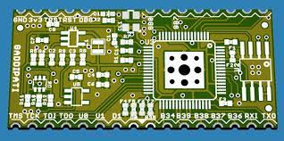
Castellated Holes or Castellations PCB are indentations formed on the edges of PCB plates in the form of semi-plated holes. These Castellations help to install one PCB board during assembly. Depending on the application, they can also appear like a small or larger part of a split circle instead of half holes. These holes have been constructed to align the boards during soldering properly. This installation procedure is performed using cast-out holes and is known as board-to-board soldering. Castellated holes are formed on various PCB modules (Bluetooth or Wi-Fi modules) and can then be used as individual parts for assembly on another board.
During the assembly process, Surface Mount Technology (THT) and Surface Mount Technology are widely used. Besides, Board-to-board soldering is used whenever a board has to be mounted on another PCB. Castellations act as a link between the module and the board on which the module is soldered.
Traditional castellation PCB Hole Process:
Drilling—–> Chemical copper—–>Panel plating–—>Image transfer——>Pattern plating—–>Striping film—–>Etching—–>Solder mask printing—–>Surface finishing—–>Castellation hole and outline milling.
The castellation PCB hole is created after round hole drilling, and the phenomenon of copper residue and copper skin twisting in the castellation hole is common, affecting the castellation hole’s function and lowering the product’s output and yield.
What is the purpose of using Castellated holes?
They can be used to duplicate some parts of a PCB circuit by drilling holes on the board edges if there is a circuit with an inverter, filter, or feedback loops, for example. These small sub-circuits can be mass-produced, tested, and soldered onto the main PCB containing the circuit’s other components as required.
The process must perform the castellation hole process steps listed below to avoid the defects mentioned above in the traditional castellation hole process.
- Drilling a hole in the substrate plate edge and a hole in the plate side.
- Plating through the hole to create a copper coating on the plate edge hole’s wall.
- Outer layer image—–>exposing—–>developing—–> second copper plating—–> Tin plating(make the hole wall covered by an anti-corrosion tin layer).
- Milling castellation holes
- Remove the anti-plating coating from the surface.
- The exposed copper on the substrate’s outer surface is removed by etching it.
- Remove the tin of castellation holes by peeling the substrate’s tin, exposing the copper of the castellation holes.
Castellation holes perfectly avoided copper residue and copper skin twist phenomenon after twice copper plating and tin plating on the substrate and were bound with copper due to the high adhesion force.
After the castellation holes are formed, the coating is etched with no copper surface oxidation to prevent residual copper or even a short circuit effectively. This challenging technology increased the printed circuit board conformance rate for small-batch urgent PCBs.
Design of Castellated Holes
The castellated holes/vias are made using standard methods, such as drilling and copper plating. Because they are cut through to create a partial or half hole to clear the path on the board edges, these holes appear as semi-circles on the board edges. Castellated PCB holes can be made in a variety of ways, including:
Castellated Holes Specifications and Recommendations
There are a few design considerations for castellated holes:
Size: Make use of the largest size available.
- Surface Finish: The board’s planned use determines this.
- Pad Design: It is suggested that you use an ENIG finish.
- Pad Size: Both the top and bottom should use the widest possible pad
- Number of Holes: The number of holes in a design is determined by design. Always aim for the smallest number of holes possible; otherwise, alignment and assembly would be difficult.
Castellated holes are used in a variety of ways.
Telecommunications, computer applications, industrial control, electricity, automobiles, and high-end consumer electronics are just a few industries that use Castellated holes on PCBs.