
General Description
The DS1302 is a low-power, trickle-current charging real-time clock chip. It contains functions like leap year compensation and can time the year, month, day, week, hour, minute, and second. The DS1302 uses extremely little power and uses less than 1mW to keep data and clock information. The following features have been added to DS1302 over DS1202: Vcc1 is a programmable trickle charge power supply, and an extra seven bytes of memory are added.
Many common serial clock circuits exist, including the DS1302, DS1307, PCF8485, and others. These circuits’ interfaces are simple, low-cost, easy-to-use, and widely used. The DS1302 real-time clock circuit has trickle current charging capabilities. The key feature is that it uses serial data transfer and uses a standard 32.768kHz crystal oscillator. It also has a programmable charging mechanism for power failure prevention and can switch off the charging function.
Telephones, fax machines, portable instruments, battery-powered equipment, and other products all employ the DS1302 chip.
DS1302 Pinout Configuration and Description
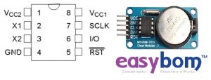
DS1302 pinout
How to Use DS1302
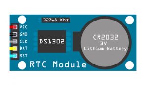
DS1302 RTC module is a high-performance, low-power, real-time clock circuit with RAM. The operating voltage is 2.0V~5.5V. A three-wire interface is used to communicate with the CPU synchronously, and a burst mode can be used to transmit a clock signal or RAM data of multiple bytes at a time. DS1302 has a 31 × 8 RAM register for temporarily storing data. DS1302 is an upgraded product of DS1202, which is compatible with DS1202, but adds dual power supply pins for the main power supply/backup power supply, and also provides the capability of trickle current charging for backup power supply.
Structure
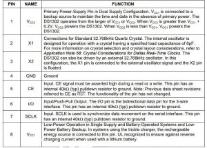
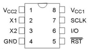
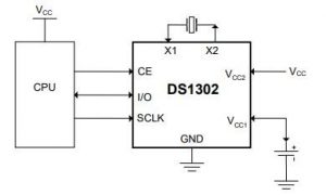
The pin arrangement of DS1302 is shown below, in which Vcc2 is the main power supply, and VCC1 is the backup power supply. It also keeps the clock running continuously even when the main power is turned off. The DS1302 is powered by the greater Vcc1 or Vcc2. When Vcc2 is greater than Vcc1, Vcc2 supplies power to DS1302. When Vcc2 is less than Vcc1, the DS1302 is powered by Vcc1. X1 and X2 are the oscillation sources, connected to a 32.768kHz crystal oscillator. RST is the reset/chip select line, which initiates all data transfers by driving the RST input high. The RST input has two functions: first, the RST turns on the control logic, allowing the address/command sequence to be fed into the shift register; second, the RST provides the means to terminate single-byte or multi-byte data transfers. When RST is high, all data transfers are initiated, allowing the operation of the DS1302. If RST is set to a low level during the transfer process, the data transfer will be terminated, and the I/O pins will become high-impedance. During power-up operation, RST must be kept low until Vcc>2.0V. RST can be set high only when SCLK is low. I/O is a serial data input and output terminal (bidirectional), which will be described in detail later. SCLK is the clock input.
Control byte
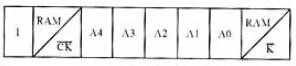
The control byte of DS1302 is shown in Figure 2. The most significant bit (bit 7) of the control byte must be logic 1. If it is 0, data cannot be written into the DS1302. If bit 6 is 0, it means accessing the calendar clock data, and 1 means accessing RAM. Data; bit 5 to bit 1 indicate the address of the operation unit; if the least significant bit (bit 0) is 0, it means to perform a write operation, and if it is 1, it means to perform a read operation, and the control byte is always output from the lowest bit.
Data flow
At the rising edge of the next SCLK clock after the control instruction word is input, the data is written into the DS1302, and the data input starts from the low bit, that is, bit 0. Similarly, the data of DS1302 is read out on the falling edge of the next SCLK pulse following the 8-bit control command word, and the data is read from low-order 0 to high-order 7.
Register
DS1302 has 12 registers, of which 7 registers are related to the calendar and clock. The data bits stored are in the form of BCD codes. The calendar, time registers, and their control words are shown in Table 1.
In addition, DS1302 has a year register, control register, charge register, clock burst register, and RAM-related registers. The clock burst register can sequentially read and write all register contents except the charge register at one time. The registers related to RAM of DS1302 are divided into two categories: one is a single RAM unit, a total of 31, each unit is configured as an 8-bit byte, and its command control word is C0H~FDH, of which odd numbers are read operations, The even number is the write operation; the other type is the RAM register in the burst mode. In this mode, all 31 bytes of the RAM can be read and written at one time, and the command control words are FEH (write) and FFH (read).
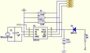
DS1302 Typical Operating Circuit
DS1302 circuit
Difference between DS1302 and DS1307
DS1302 VS DS1307
DS1302 is a semi-SPI interface
At the rising edge of the next SCLK clock after the control instruction word is input, the data is written into the DS1302, and the data input starts from the low bit, that is, bit 0. Similarly, the data of DS1302 is read out on the falling edge of the next SCLK pulse following the 8-bit control command byte, and the data is read from low-order 0 to high-order 7. During data transfer from the DS1302’s clock calendar or RAM, the DS1302 must first send a command byte. If a single-byte transfer is performed, after the 8-bit command byte is transferred, the data byte is input on the rising edge of the next 2 SCLK cycles, or the data byte is output on the falling edge of the next 8 SCLK cycles.
Circuit diagram of DS1302 connected to CPU:
DS1307 is an I2C interface
DS1307 is a slave device on the I2C bus, the address is fixed as “11010000”, DS1307 write operation TWI is controlled to receive mode, the master device writes data to the DS1307 register or internal RAM in the following order:
Step 1: START signal,
Step 2: Write SLA+W (0xd0) bytes, DS1307 responds (ACK),
Step 3: Write a 1-byte memory address (the first byte written in the fourth step below will be stored in this address in the DS1307), the DS1307 responds,
Step 4: Write data (multiple bytes can be written after each byte is written, the internal address counter of DS1307 increases by one, and DS1307 responds),
Step 5: STOP signal.
Circuit diagram of DS1307 connected to CPU:
DS1302 Datasheet Download
The DS1302 Datasheet gives an elaborate introduction to it, which is able to help you avoid some unnecessary problems when using it.
Conclusion
Many DS1302 RTCs have low clock accuracy, because the selected crystal oscillator is easily affected by the environment, and there are disadvantages such as clock confusion. DS1302 can be used for data recording, especially for some data points with special significance, which can realize the simultaneous recording of data and the time when the data appears. This kind of record is of great significance to the analysis of long-term continuous measurement and control system results and the search for the cause of abnormal data. The traditional data recording method is interval sampling or timing sampling. There is no specific time record. Therefore, only the data can be recorded but the time of its occurrence cannot be accurately recorded. If the microcontroller is used for timing, on the one hand, a counter needs to be used, which occupies hardware resources. On the other hand, it is necessary to set interrupts, queries, etc., which also consumes the resources of the microcontroller, and some measurement and control systems may not allow it. However, if the clock chip DS1302 is used in the system, this problem can be solved very well.
All in all, it is necessary for electronic engineers and enthusiasts to read the article provided by Easybom carefully.