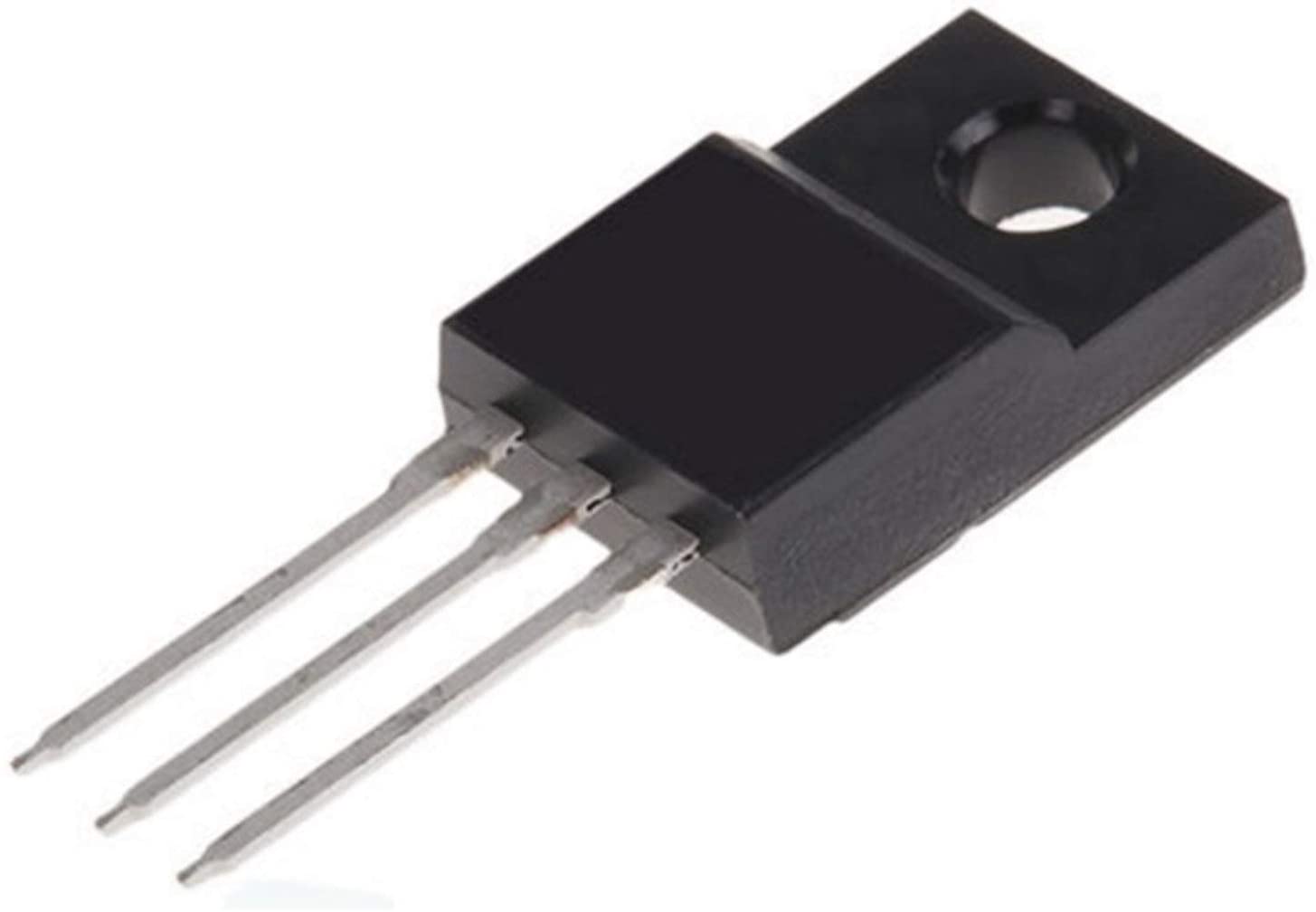
A bipolar transistor is a triode. The simplest distinction is: the three poles are called collector, base, and emitter. It is also a bipolar transistor. Because the unipolar tube does not use such a name. The unipolar tube is called the source, the gate, and the drain.
What is a Bipolar Transistor?
Bipolar transistor, the full name is bipolar junction transistor. It is commonly known as a triode, which is an electronic device with three terminals. Bipolar transistors are a groundbreaking invention in electronic history.
The function of this kind of transistor is the circulation of electron and hole carriers simultaneously. It is called bipolar, also called bipolar carrier transistor. It works differently from unipolar transistors such as field-effect transistors. The latter’s working mode only involves the drift effect of a single type of carrier. The PN junction forms the boundary between two different dopant aggregation regions.
Basic Principles of Bipolar Transistors
It is the NPN kind of bipolar transistor that may be thought of as two diodes having common anodes joined. When the bipolar transistor is operating properly, the base-emitter junction (we call this PN junction the “emitter junction”) is in a positive bias state. The base-collector (we call this PN junction the “collector junction”) is in a reverse-biased state. When there is no applied voltage, the electron concentration in the N region of the emission junction is greater than that in the P region, and part of the electrons will diffuse to the P region. One of the holes in the P zone will also spread to the N area. A space charge region will be formed on the emitter junction. It generates an internal electric field. It goes from the N area to the P area. The electric field can prevent the occurrence of the mentioned diffusion process, allowing for the creation of equilibrium in the dynamic. At this time, if a forward voltage is applied to the emission junction, the dynamic balance between carrier diffusion and the internal electric field in the depletion layer will be broken. This will cause thermally excited electrons to be injected into the base area. The base region of NPN transistors is P-type doped. Here, holes are mostly doped substances. Therefore, electrons in this area are called “minority carriers”. In the field of bipolar transistors, the area of the region that is called base typically is only a few tenths micrometer. What we need to pay attention to is that although the collector and emitter are both N-type doped, the degree of doping and physical properties of the two are not the same. We must distinguish the form of a bipolar transistor in which two diodes in opposite directions are connected in series.
Structure of Bipolar Transistor
A bipolar transistor is comprised of three doped semiconductor regions. They include the emitter region as well as the base region and finally, the collector. These regions are respectively N-type, P-type, and N-type semiconductors in NPN-type transistors. In PNP-type transistors, they are P-type, N-type, and P-type semiconductors. Each semiconductor area has a pin termination, usually with letters E, B, and C to represent Emitter, Base, and Collector.
When bipolar transistors are connected via the emitter connector tiny variations in the voltage applied to both the emitter and base will result in significant changes in the current that flows between the collector and the emitter. Using this property, we can amplify the input current or voltage. Use the base of the bipolar transistor as the input. The collector serves as the output terminal. Using the principle of equivalent, a bipolar transistor can be regarded as a voltage-controlled current source, or it can be regarded as a current-controlled voltage source. In addition, looking in from the left side of the two-port network, the input impedance at the base is reduced to that of the base resistance. This reduces the requirements for the load capacity of the previous-stage circuit.
More information on bipolar transistor models is available easybom!
