What are FinFETs?
When it comes to FET, people who study electronics are familiar with it. FET (field-effect transistor) is a common three-port semiconductor device, and the more common ones are JFET (junction field-effect transistor) and MOSFET (metal oxide field effect transistor). The following figure shows the working schematic diagram of a common FET.
So what exactly are FinFETs?
The full name of FinFET is the fin field-effect transistor, which is a new complementary metal-oxide-semiconductor transistor. FinFET is an innovative technology derived from the traditional standard transistor – the field-effect transistor. In the traditional transistor structure, the gate that controls the passage of current can only control the turn-on and turn-off of the circuit on one side of the gate, which belongs to a planar structure. In the structure of FinFET, the gate has a fork-shaped 3d structure similar to a fin, which can control the on and off of the circuit on both sides of the circuit. This design can improve circuit control and reduce leakage current, and can also greatly shorten the gate length of the transistor.

FinFET Structure and Operation
FinFET vs MOSFET
The main difference between the FinFeT structure and the planar MOSFET structure is that its channel is composed of high and thin fins raised on an insulating substrate, the source and drain electrodes are at its two ends, and the tri-gate is close to its sidewalls and tops for auxiliary current control. This fin-shaped structure increases the surface of the gate surrounding the channel and strengthens the control of the gate to the channel, which can effectively alleviate the short channel effect in planar devices, greatly improve circuit control and reduce leakage current, and greatly shorten the gate length of the transistor. Because of this characteristic, FinFET does not need a highly doped channel, so it can effectively reduce the scattering effect of impurity ions and improve the channel carrier mobility.
The main feature of FinFETs is that the channel region is a fin-like semiconductor surrounded by a gate. The length of the fin along the source-drain direction is the channel length. The gate-wrapped structure enhances the control ability of the gate and provides better electrical control for the channel, thereby reducing leakage current and suppressing the short-channel effect. However, there are many types of FinFETs, and different FinFETs have different electrical characteristics. The following descriptions are given according to the type of substrate, the direction of the channel, the number of gates, and the structure of the gate.
FinFETs can be divided into two types according to the FinFET substrate. One is SOI FinFET and the other is bulk FinFET. FinFETs are formed on bulk silicon substrates. Due to different fabrication processes, bulk silicon substrates have the advantages of low defect density and low cost compared to SOI substrates. In addition, due to the low thermal conductivity of the buried oxide layer in the SOI substrate, the heat dissipation performance of the bulk silicon substrate is also better than that of the SOI substrate. Buk FinFET and SOI FinFET have similar parasitic resistance, parasitic capacitance thus can provide similar power performance in the circuit. However, lightly fin-doped FinFETs on SOI substrates, compared to Buk FinFETs, exhibit lower junction capacitance, higher mobility, and electrical performance of voltage gain.
How good is FinFET?
For field-effect transistors, the most commonly used is MOSFET (the full name is metal oxide semiconductor field-effect transistor). The MOSFET was first implemented successfully in 1960 by D. Kahng and Martin Atalla of Bell Labs. Its operation principle is completely different from the bipolar junction transistor, BJT which is created by William Shockley in 1947. Because of the advantages of low manufacturing cost, small area, and high integration, they are widely used in large-scale integrated circuits (LSI) or very large-scale integrated circuits (VLSI), and the importance is far more than BJT.
But, the development of MOSFET has been around for over 60 years. As semiconductor technology advances, technology, the limitation of MOSFET’s capabilities is becoming more apparent. We are aware that in MOSFETs the gate length is around 10 nanometers that is one of the most tiny, and the most difficult to construct of all structures. Therefore, we typically employ the length of the gate to indicate the progression in the process which is known as processing linewidth. The length of the gate will decrease as the process advances in technology, ranging from 0.18 microns to 0.13 microns at the beginning stage to 90 nanometers 65 nanometers, 45 nanometers 22 nanometers and the newest technology will be 10 nanometers. The shorter the length of the gate is the smaller the whole MOSFET is in addition, the more compact the device that houses millions of MOSFETs is and the smaller the circuit is after packaging. In addition, the mobile phone is much smaller!
How small is 10 nanometers? Bacteria weigh about one micrometer, while viruses measure around 100 nanometers. That’s right, modern technology is capable of creating structures that are just one-tenth (10 nanometers) of viruses. Awesome!
But, when the length of the gate is decreased by less than nanometers and there are many issues to be faced. Most problematic is when the length of the gate is shorter and the distance between the drain and source is shorter and the oxide beneath the gate is thinner electrons can pass through and cause leakage. Another issue that is more difficult to solve, is whether electrons are able to move between the source and drain, is controlled by the gate voltage. However, the shorter the length of the gate, the smaller the area of contact between the source and the channel (the red-dotted area in the image below) and the less impact of the gate’s effect upon the channel. What can we do to maintain the influence of the gate (contact zone) in the channel?
So, three professors, including Hu Zhengming, Tsu-Jae King-Liu as well as Jeffrey Bokor of the University of California, Berkeley, developed the fin field effect transistor (FinFET) which transformed the initial 2D MOSFET into 3D as seen in the image. Fin is the name given to it. Fin because its design is reminiscent of a fish’s fin.
It is evident from the diagram that the source as well as the drain get pushed up into a three-dimensional plate to ensure that the channel that connects the source and drain is transformed into a plate, and the area of contact between the source and channel gets bigger. (The region in which it is seen that the blue oxide on the image below comes into contact with the bottom is clearly greater than the red-dashed area shown in the previous figure) Also, even if the gate’s length is decreased by less than 20 nanometers there is a substantial contact area maintained, which is able to regulate the flow of electrons through the channel from source. This way, the current can be more precisely controlled as well as loss of power and leakage is reduced in the process. Dynamic power consumption refers to the energy used when the FinFET is changed between 0 and 1 or changes from 1 to 0. The reduction in leakage and dynamic power consumption means it will conserve more energy!
FinFET is the solution to cutting the length of the gate down by less than 20nm. Only by using the patents and technology of this technique can we ensure future technological advancements in the semiconductor industry.
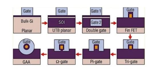
Naturally FETs don’t remain permanent, and FinFETs may not be the only alternative, and their evolution is ongoing. In the past seventeen years CMOS technology has seen significant advancements with respect to the materials used in the construction and manufacturing industries. The first big step was introduced by strain engineering in the 90nm technology node. The next step is metal gates that have 45nm high-k dielectrics and FinFET designs at the 22nm node. 2012 marked the beginning of FinFET, the first commercial FinFET with a 22nm wavelength. Further enhancements to the FinFET architecture have led to increased performance as well as reduced the surface. FinFETs’ 3D design provides many benefits, like an increased fin height to allow for a more drive current, all within an identical footprint. Below is a diagram of the development of MOSFET structures like triple gate, double gate, pi gate omega gate and gate around. Tri-gate and dual gate FinFETs are widely used because of their simplicity and easy fabrication. Even though GAAFETdevices had been first proposed prior to FinFETs but the latter are more suitable for implementation.
SOI and FinFET
Below, Easybom will discuss two new MOS structures, SOI and FinFET. The main goal of using both structures is to maximize gate-to-channel capacitance and minimize drain-to-drain channel capacitance.
1. Silicon on insulator (SOI)
The main difference between traditional MOS structures and SOI MOS structures is that SOI devices have a buried oxide layer that isolates the base from the substrate. As shown in the figure, the SOI transistor is a planar structure.
The manufacturing process of SOI MOS is similar to the bulk MOS (traditional MOS) process outside the starting silicon wafer. SOI wafers have three layers: 1. A thin surface layer of silicon (which forms the transistors); 2. An underlying layer of insulating material; 3. Support or “handling” of the silicon wafer.
The basic idea of buried oxide is to reduce parasitic junction capacitance. The smaller the parasitic capacitance, the faster the transistor operates. Due to the BOX layer, there is no leakage path away from the gate, which results in lower power consumption.
Generally, SOI devices are classified as partially depleted (PD) SOI and fully depleted (FD) SOI. Compared with PD-SOI, FD-SOI has a very thin bulk structure and thus is completely depleted during operation. FD-SOI is also known as ultra-thin body SOI. For PD-SOI, the bulk is 50nm~90nm thick. For FD-SOI, the body thickness is about 5nm~20nm.
Advantages of SOI devices:
Drain/source parasitic capacitance is reduced due to oxide layer isolation. As a result, the device has lower latency and dynamic power consumption compared to bulk CMOS.
Due to the oxide layer, the threshold voltage is less dependent on the back gate bias compared to bulk CMOS. This makes SOI devices more suitable for low-power applications.
SOI devices have better subthreshold characteristics and less leakage current.
SOI devices do not have latch-up issues.
Disadvantages of SOI devices:
One of the disadvantages of PD-SOI devices is that they have a historical effect. In PD-SOI, floating bodies are evident as the body thickens. Therefore, the bulk voltage depends on the previous state of the device. This floating body voltage can change the threshold voltage of the device. This can lead to a significant mismatch between two identical transistors.
Another problem with SOI devices is self-heating. In SOI devices, the active thin body is on silicon oxide, which is a thermal insulator. During operation, the power consumed by the active area cannot be easily dissipated. As a result, the temperature of the thin body increases, which reduces the mobility and current of the device.
One of the challenges of FD-SOI is the difficulty of fabricating thin SOI wafers.
2. FinFET
Hu Zhengming, the chief technology officer of TSMC and a former professor at Berkeley, and his team proposed the concept of FinFET in 1999 and proposed UTB-SOI (FD SOI) in 2000. The main structure of these two structures is the thin body, so the gate capacitance is closer to the whole channel, and the body is very thin, about 10nm or less. So there is no leakage path very far from the gate. The gate effectively controls leakage.
The basic structure of their proposed FinFET is a channel controlled by multiple channels. One of the double gate structures is shown in the figure.
Double gate structure
Modern FinFETs are three-dimensional structures, as shown in the figure below, also known as tri-gate transistors. FinFETs can be implemented on bulk silicon or SOI wafers. This FinFET structure consists of thin (vertical) fins of silicon bulk on a substrate. This channel provides good three-sided control of the channel around the channel. This structure is called a FinFET because its Si body resembles the back fin of a fish.
Fin-FET structure
In bulk-MOS (planar structure MOS), the channel is horizontal. In a FinFET channel, it is vertical. So for FinFETs, the height of the channel (Fin) determines the width of the device. The perfect width of the channel is given by the equation.
Channel Width = 2 X Fin Height + Fin Width
The drive current of the FinFET can be increased by increasing the width of the channel, i.e. by increasing the height of the fin. The device drive current can also be increased by constructing multiple fins connected together in parallel as shown in the figure. This means that for FinFETs, the channel width is not arbitrary as it is always a multiple of the fin height. Therefore, the effective width of the device is quantized. In the planar structure, the drive strength of the device can be freely selected by changing the channel width.
Multi-fin FinFET structure
In conventional MOS, doping is inserted into the channel to reduce various SCEs and ensure high Vth. In FinFETs, the gate structure is wrapped around the channel and the body is thin to provide better SCE, so channel doping is optional. This means that FinFETs are less affected by dopant-induced changes. Low channel doping also ensures better mobility of carriers within the channel. Therefore, the performance is higher. One thing to note here is that both FinFET and SOI technologies have body thickness as a new scaling parameter.
FinFET technology offers many advantages over bulk CMOS, such as higher drive current for a given transistor duty cycle, higher speed, lower leakage, lower power consumption, no random dopant fluctuations, so transistor mobility and size are better, beyond 28nm.
SOI vs FINFET
Since SOI technology is very close to planar bulk silicon technology, there is no need for much investment in Fab. Therefore, existing bulk technology libraries can be easily converted to SOI libraries. Another benefit of SOI over FinFETs is good back gate biasing options. Vt can be controlled by creating a backdoor area under the BOX. This makes it suitable for low-power applications.
The main limitation of SOI technology is that the cost of the wafer is higher than that of bulk silicon because it is very difficult to control the tin-silicon film over the entire wafer. Another stumbling block for SOI promotion is the limited number of SOI wafer suppliers. According to Intel, SOI wafers account for about 10 percent of the total process cost.
FinFET has a higher drive current compared to SOI. Furthermore, in FinFETs, straining techniques can be used to increase carrier mobility.
One of the disadvantages of FinFETs is their complex manufacturing process. FinFET manufacturing costs 2-3% higher than bulk silicon, according to Intel.