General Description
The Microchip AT24C02C is a two-kilobyte serial EEPROM with an I2C (2-wire) serial interface. The device is arranged as a single 256 x 8 block and is designed for consumer, industrial, and automotive applications that require stable nonvolatile memory storage. The EEPROM can be packaged in a variety of ways to save space.
AT24C02C Series Features
- Integrated Schmitt triggers to reduce input spikes and noise
- Using a plain I2C compatible 2-wire digital serial interface
- Bidirectional input/output pin for transferring data
- High durability and reliability in the manners of 1,000,000 write cycles and data retention
- Green package method provided
- Wide temperature range for industrial application
- Random and sequential read provided
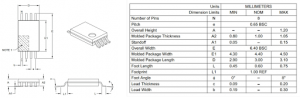
AT24C02C Package Dimension (TSSOP)
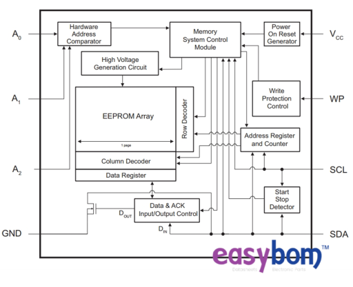
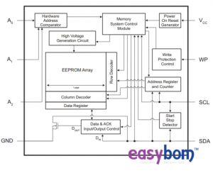
AT24C02C-PUM Block Diagram
Instructions
Applications of AT24C02C Series
The AT2402C series I2C EEPROM allows for values to be written and stored for long periods of time while using very little power. They are commonly applied in most situations that require interfacing with MCU and is also suitable for battery-operated devices.
How to Use AT24C02C
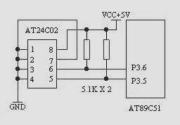
Pin 1, 2, and 3 of the AT24C02 in the figure 1 are three address lines, which are used to determine the hardware address of the chip. They are all grounded on the AT89C51 test development board, and the 8th and 4th feet are positive and negative power supply, respectively. The fifth foot SDA is serial data input / output, and the data is transmitted serially through this bi-directional I2C bus, which is connected with the P3.5 of the single-chip microcomputer on the AT89C51 test development board. The sixth foot SCL is a serial clock input line, which is connected with the P3.6 of the single chip microcomputer on the AT89C51 test development board. Both SDA and SCL need to be pulled up with a resistance of 5.1K between the positive power supply and the positive power supply. Foot 7 needs to be grounded.
There is an on-chip address register in 24C02. After each byte of data is written or read out, the address register is automatically added to 1 to read and write to the next memory unit. All bytes are read in a single operation. To reduce the total write time, up to 8 bytes of data can be written in a single operation.
User Guidelines
– Page Write
Following each data word, the bottom three bits of the word address are internally increased. The memory page row position is retained since the upper order address bits are not increased. Regardless of the amount of bytes actually written, Page Write operations are limited to writing bytes within a single physical page.
The address counter will “roll-over” to the beginning of the same page when the increased word address hits the page boundary. Creating a roll-over event, on the other hand, should be avoided since previously loaded data on the page may be updated accidentally.
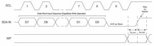
– Write Protect Setup and Hold Timing
As indicated in Figure 2, the WP pin state must be legitimate with regard to the corresponding setup (tSU.WP) and hold (tHD.WP). The WP setup time is the length of time before the Stop condition is given that the WP state must be stable. The WP hold time is the period of time that the WP must remain steady following the Stop condition.
– Device Reset
The system designer must guarantee that instructions to the device are not transmitted until the VCC supply has stabilized at a level greater than the minimum VCC level. Furthermore, after the VCC has above the minimum VCC level, the bus Master must wait at least tPUP before delivering the device the first command. The values associated with these power-up settings may be found in Table 1.
![]()
(Summarized by Easybom)
Datasheets
https://pdf.easybom.com/r/datasheets/microchip-at24c02cpum-datasheets-3357.pdf
Similar Parts
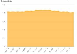
Market Quotation
Popularity across the World

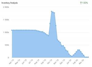
Stats Analysis