Surface mount technology has been developed to reduce manufacturing costs and it also makes more efficient use of PCB space.SMT, as it’s known in the industry, was created by decreasing size from through-hole assembly with greater automation than ever before possible due to surface mount components on top instead – reducing overall labor needed for each step during the production process too!
So, today we will take a deep look into the surface mount soldering PCB Assembly Process and cover each step that goes into the production and assembly of printed circuit boards.
What Is THe SMT PCB Assembly Process?
Well, it’s not as difficult to understand as you might think. This method of manufacturing involves placing components onto an electronic board using automatic machines and then soldering them together at each stage in order to create finished products with fewer errors during production that can last longer than any other design available today! In this blog, we’ll go over what exactly occurs during a typical PCB assembly process for small electronic cards and how those steps can be automated with machines!
-
Design And Layout Phase:
In the design and layout phase, initial SMT PCB layouts are created by using CAD software packages such as EasyEDA or EagleCAD.
-
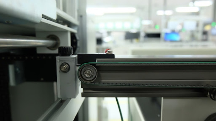
Preparing Gerber/CAD To Centroid/ Pick & Place Files
There is a lot that goes into preparing Gerber/CAD files to be used with manufacturing. First, you have the design and layout of the initial PCB complete in order for it to run smoothly; however, there are also various machines set up depending on what type of SMT process will need them, such as pick & place or soldering etc.
-
PCB Material Examination And Stencil Preparation
PCB material examination and stencil preparation is an essential step in the production process. The technician determines whether there are any flaws in your design, as well as prints out solder paste for each individual pad position using a template or “stencil.”
-
Solder Paste Printing
Solder paste is a mixture of flux and tin that gets connected to SMC pads on the PCB through stenciling, squeegees, or even jets. This standard method is used for small-scale production but jet printing has increased popularity over time because it can be done in larger batches than traditional methods with less equipment needed at one go – saving cost as well!
-
SMC Part Placement
The assembled Printed & SPI inspected PCBs then move on to the next part of the manufacturing process, which is mounting SMC parts. Many factory SMT machine operations utilize pick and place machines, which use the vacuum or gripper nozzles as well as high-speed positioning systems in order to place components at preprogrammed locations with great accuracy securely– after this step, all that’s left before reflow soldering occurs are checks by automated optical inspection equipment like what you might find within most factories today.
-
Reflow Soldering
Reflow soldering is a popular and reliable way to make electrical connections between SMC parts, which are then mounted onto the PCB. This process involves heating both pieces so that solder flows from its tip into either side of an insertion point on one component or wire end; this makes it possible for them all to connect together through some uniform physical connection like your circuit board!
-
Post-Reflow AOI
After finishing the reflow soldering process, boards go through another AOI inspection to ensure that no mistakes were made and determine if solder joint quality meets expectations.
-
Cleaning The Finished Board
This step is done by almost all Chinese PCB manufacturers. When the SMT PCB board is finished assembly, it’s time for one last step. First, a thin layer of flux will be applied and completely covered by plastic to ensure good contact between components while soldering begins; then, we wipe off any excess residue with iso-propyl alcohol wipes before finally wiping down our final product from all sides until it shines like new!